In the infrared spectrum, the current optoelectronic devices rely on two main types of detectors, the Quantum and the Energy detectors. The Quantum detectors are fast but requires very low temperature cooling. They are based on narrow band-gap semiconductors such as InSb and HgCdTe. Because of cryogenic operating conditions, quantum detectors are dedicated to high performance needs (defense, astronomy applications). Alternatively, energy detectors such as bolometers can detect infrared light at room temperature but at a price of a longer response time. There is nevertheless a growing demand for IR detectors in application fields such as building thermal management or night assistance for driving. These new applications require a radical cost reduction that current quantum technologies are unlikely to bring. Recently, flexible, transparent graphene based photodetectors have been a topic of great interest due to their fast response time (on the order of 10-8 ms) and light absorption capability in a broad range of wavelengths covering the ultraviolet to far-infrared and THz regime. However, the low light absorbance and the absence of gain mechanism due to fast recombination of photogenerated electrons and holes lead to a low responsivity (~1 A/W) in graphene photodetectors.
This highlight shows the first results, obtained in a new collaboration between Leti/SMTP and our laboratory, on a new family of low cost near infrared photodetectors based on graphene/nanoparticles (PbS quantum dots) hybrids (Fig. 1A).
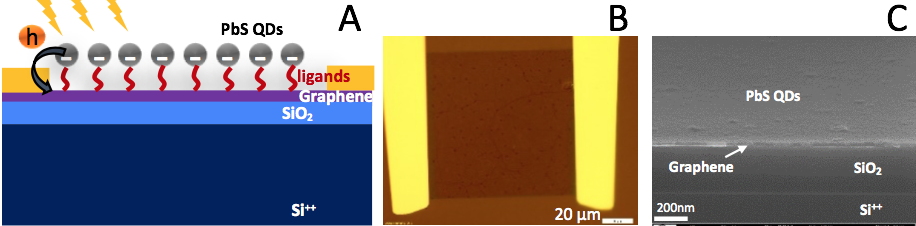
Figure 1: A) Schematic diagram of the PbS QDs-graphene hybrid photodetector along with the circuit diagram for optoelectronic measurements. B) CVD-grown graphene FET. C) Cross-section SEM image of the homogeneous PbS QD film deposited on graphene.
The concept of these photodetectors, first proposed in the literature in 2012, is to decouple transport and absorption. The basic idea is to take advantage of the large mobility of graphene and the efficient and tunable absorption of colloidal PbS quantum dots (QDs) in the IR. Light absorption thus occurs within the semiconductor QDs and due to selective charge transfer a current can flow within the graphene layer.
Commercial graphene FETs (Field Effect Transistors) on SiO2 (90 nm)/Si wafers were used as the base of the photodectors (Fig. 1B). 2.8 nm colloidal PbS QDs with an excitonic peak at 875 nm were synthesized in organic solvent at 100°C. A controlled layer-by-layer deposition using an automated dip-coating process was developed to coat the graphene-FET with a homogeneous layer of ~100 nm of QDs (Fig. 1C). Functionalization of the graphene surface as well as surface ligand exchange and passivation of the QDs with appropriate molecules were required to obtain crack-free films of high conductivity.
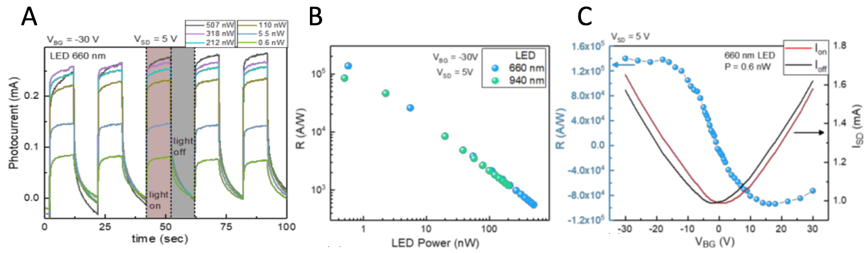
Figure 2: A) Photoresponse of the graphene/PbS hybrid device under illumination at 660 nm for different values of irradiation power. B) Responsivity R (Iphotocurrent/P) as a function of irradiation power at 660 nm and 940 nm. C) Responsivity R vs VBG showing positive and negative photoresponse in the hole doped and electron doped region of graphene, respectively.
Optoelectronic measurements were performed using a probe station at 300 K under high vacuum (~10
6 mbar) with LEDs of 660 nm (visible) and 940 nm (infrared) as light sources. The photoresponse of the developed graphene photodetector (100 µm channel length) is shown in Fig. 2A, demonstrating the increase of the photo-response with irradiation power P. The responsivity R of the device (R = IP / P) increases with decreasing P as expected (Fig. 2B). We measured a responsivity as high as 1.4×10⁵ A/W corresponding to a photoconductive gain of ~ 108 at low excitation power P = 0.6 nW for two different wavelengths (660 nm and 940 nm). These first results are very competitive in view of the state-of-the-art, and serve as a solid basis for further developments.
By varying VBG (Fig. 5c), we observe that the responsivity of our device can be tuned (reversed in sign and switched off electrically by tuning the gate), which is an attractive feature for developing tunable photodetectors for imaging applications. Further analyses of the novel hybrid IR photodetectors are underway, and an improvement of their response time is targeted via optimization of the QD surface chemistry. The final goal will be the development of low-cost, fast and efficient SWIR photodetectors, working in particular in the 1.3-1.5 µm spectral range.