The concept originated in 2005 from the need for measurements of local electronic properties in organic materials for the future: conjugated polymers, blends, hybrid systems. At that time, a few labs had developed nanostencils, but the coupling with the AFM required highly technical know-how. Routine service was thus almost impossible, especially because the most classical detection method was used: the deflection of a laser beam focused on the AFM tip.
However, our lab masters the technique of the tuning fork, which is a resonator and a self-sensor for the AFM. We therefore built our project on this basis and mounted a chip with the stencil and the AFM tip on one branch of the fork (a configuration called QPlus.)
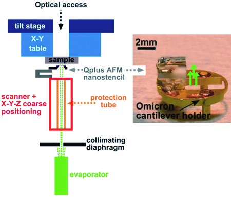
Figure 1: The evaporator/fork/mask system.
Theoretical and practical approach We thus launched two major tasks: i) fabrication of the system evaporator / fork / mask ii) integration into the AFM. The device consists of (Figure 1):
- an evaporator and a collimating diaphragm
- a piezoelectric scanner tube driving the fork, drilled in its center to let out evaporated molecules or atoms
- the tuning fork - a silicon-based chip with a structured Si
3N
4 membrane, part of which contains the stencil - an integrated AFM tip
- an X-Y closed loop nano-positioning table for wide field imaging.
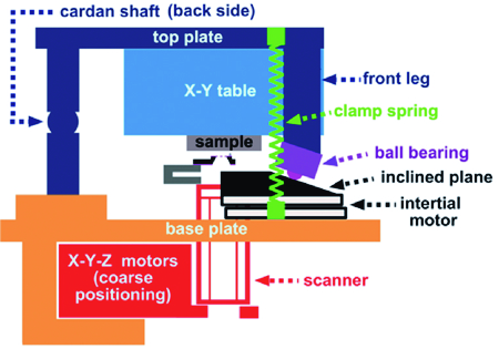
The masks were etched by Leti. The modeling of QPlus vibrational modes in every configuration was performed by Iramis. The mechanical developments were done entirely by Lemoh (Figure 2). All had to meet the requirements of AFM imaging (wide field, high resolution, accuracy in (re)positioning), of static and dynamic design of electrodes (Figure 3). The high precision of the AFM control stage is used to position the mask relative to the surface. Better than 1% parallelism is routinely obtained.
|
Figure 2 | |
Figure 3 |
| | |
 | |
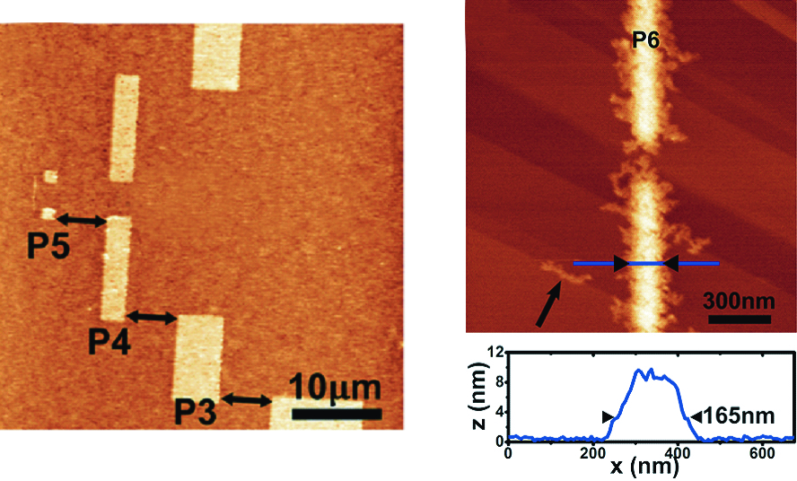 |
Figure 2: The nanostencil integrated in the AFM housing.
Figure 3: Examples of performance in simple mode (pattern imaging with a separate probe) and combined mode (imaging with the tip integrated in the nanostencil).
Performance We have experimentally demonstrated that, despite the addition of a massive chip on the fork, high-resolution imaging (about 10 nm) is possible on a wide range of samples, including soft materials. Spectroscopic measurements show that the AFM control processes are fully efficient. The AFM tips made by focused ion beam (FIB) appear well suited, both for topographic imaging and spectroscopy. The positioning of the probe is reproducible to a few tens of nanometers after a trip of several tens of microns. The simultaneous evaporation of patterns in the micrometer (several hundred µm²) and nanometer range is possible, either in static, dynamic or sequential mode. To date, patterns that are 165 nm-wide have been obtained in dynamic mode. While breaking thinness records is not the primary need, we can however reduce this size by optimizing the distance between the surface and the membrane. Gold, silver or C60 were deposited under high vacuum at a speed of 0.1 to 1 nm per minute.
New implementation project Although nanoelectronics (organic transistors) and optoelectronics were originally the main objectives, new needs have emerged, for example for organic photovoltaics. A new project supported by the DSM-Energy program involves model planar junctions. The project benefits from the laboratory know-how in synthesis of thin-film organic single crystals (hole conducting materials). The QPlus nanostencil is used for the deposition of C60 (electron conductor) and of the cathode, and for the measurement of both cell performance under illumination and intrinsic properties (mobility) of the components (Figure 4.) We thus have a flexible way of fabricating and studying multiple samples without using lithography at any step.
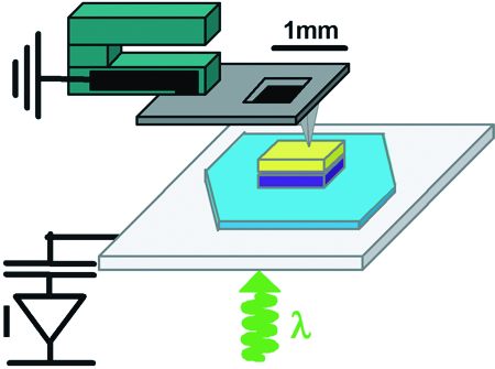
Figure 4: Planar junction for organic photovoltaics. The organic single crystal (blue) is deposited on the ITO and glass transparent anode. The C60 (purple) and the aluminum cathode (yellow) are evaporated through the stencil. Several cells of this type (varying thicknesses and sizes) have been produced and characterized on a unique single crystal.