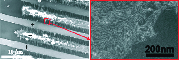
We proceeded in three steps. First of all, we synthesized chemically colloidal nanostructures of CdSe. The obtained nano-objects – for example 80-nm long and 8-nm large rods – present an intrinsic shape anisotropy. Second, we prepared inter-digitalized electrodes by optical lithography. Third, we put a drop of the CdSe nanorod colloidal solution on the electrodes while applying an electric field. The nanorods orient themselves between the electrodes due to their permanent dipole moment.
However, by shining UV light on the nanorods, they can be directed in a much more efficient way: as photo-excitation enhances the dipolar character of the nanorods, their orientation in the electric field is considerably improved. Micrometric bridges are visible between two adjacent electrodes (Figure). Hence our technique of "electro-optical" assembly allows us to control the localisation of semiconductor nanorods and to contact them electrically. At the same time these nano-objects emit polarised light, which makes them attractive materials for optoelectronics. This work has been done in collaboration between SPrAM and LTM (CNRS).